Design & specifications
If you want to know how BeagleV-Fire board is designed and what are it’s high-level specifications then this chapter is for you. We are going to discuss each hardware design element in detail and provide high-level device specifications in a short and crisp form as well.
Tip
For hardware design files and schematic diagram you can checkout BeagleV-Fire GitLab repository: https://git.beagleboard.org/beaglev-fire/beaglev-fire
Block diagram
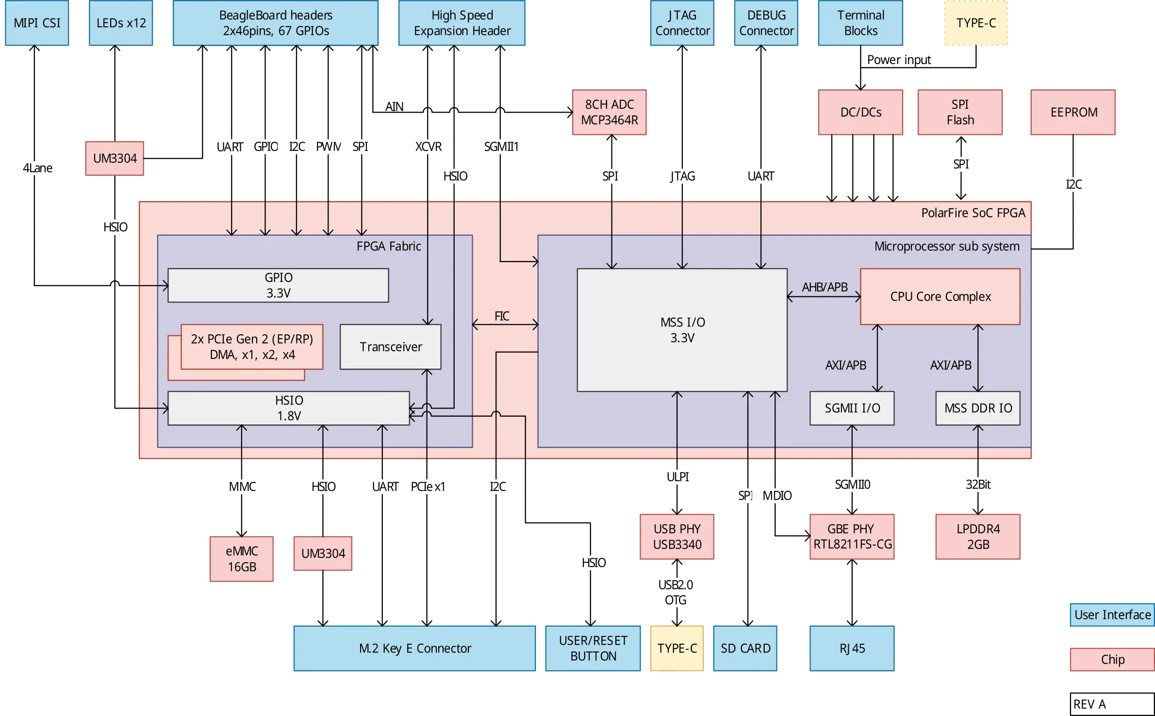
Fig. 255 System block diagram
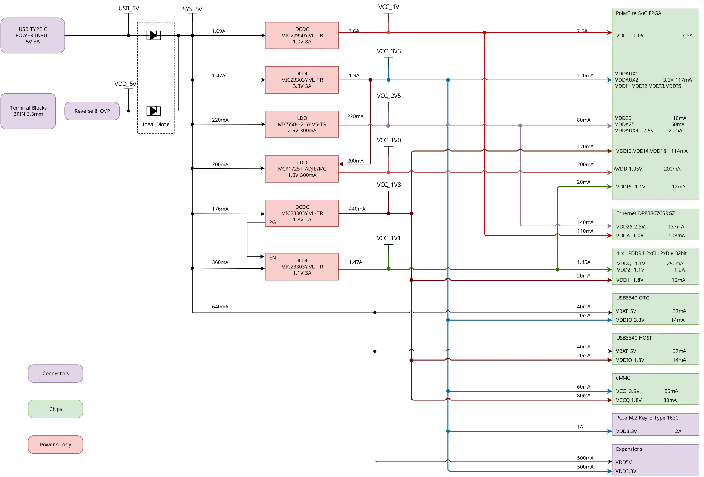
Fig. 256 Power tree diagram
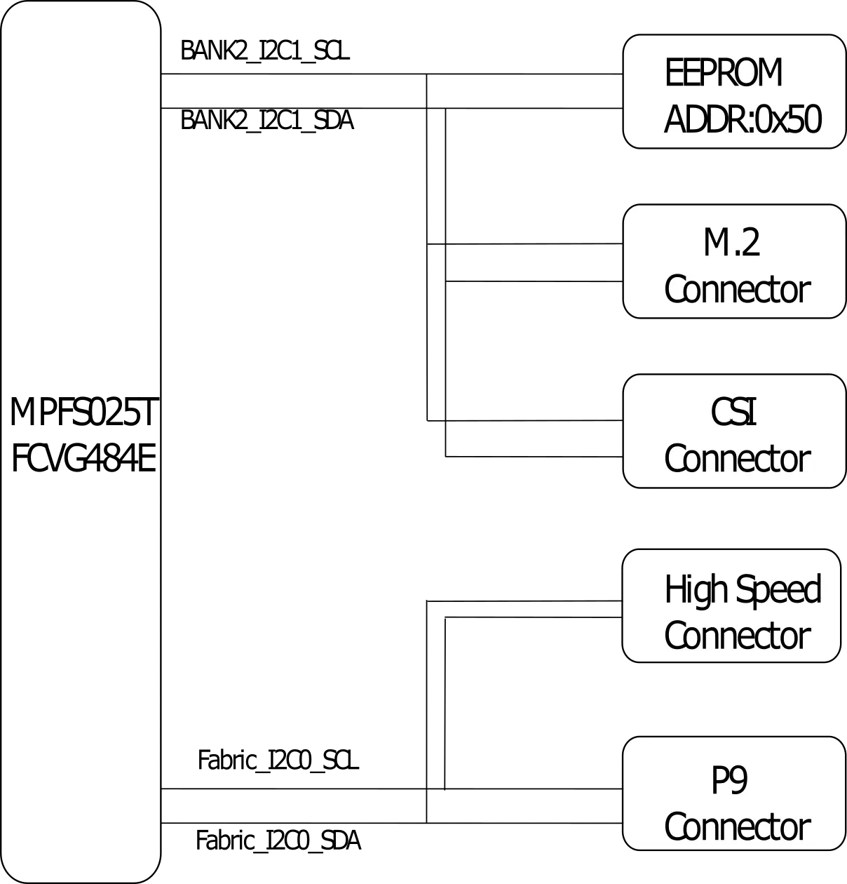
Fig. 257 I2C tree diagram
System on Chip (SoC)
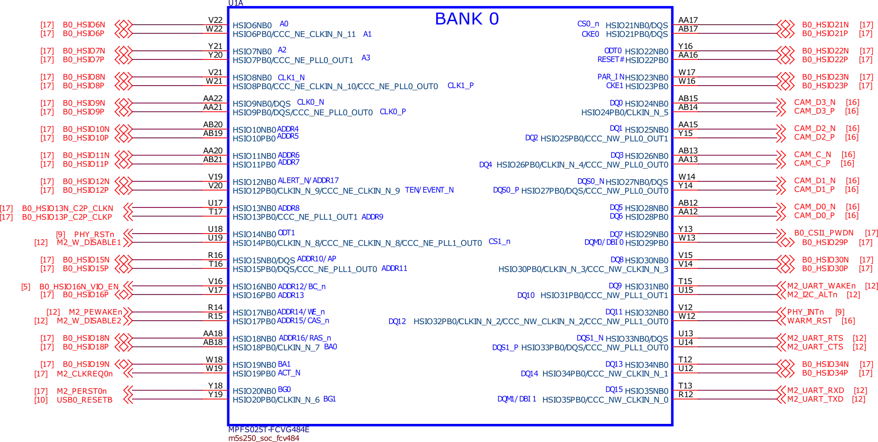
Fig. 258 SoC bank0
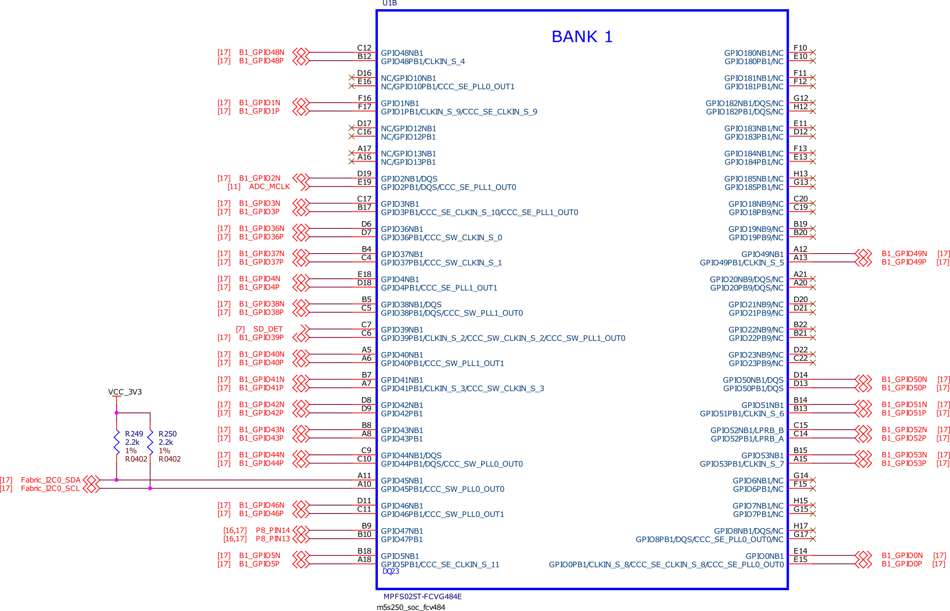
Fig. 259 SoC bank1
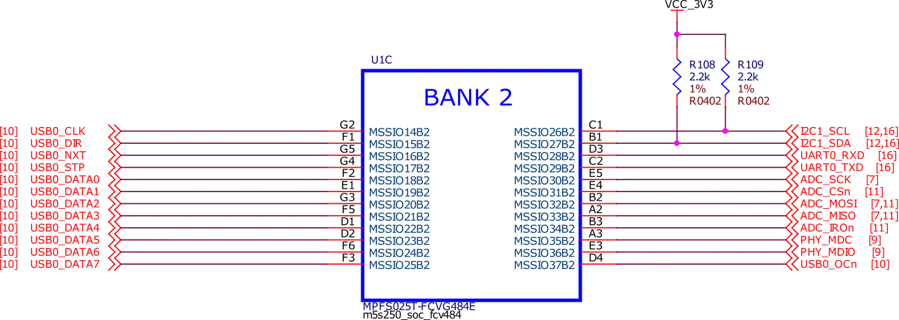
Fig. 260 SoC bank2
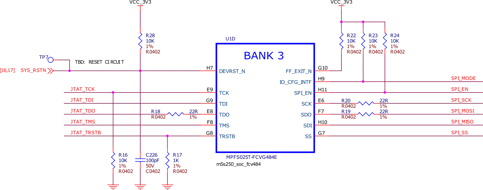
Fig. 261 SoC bank3
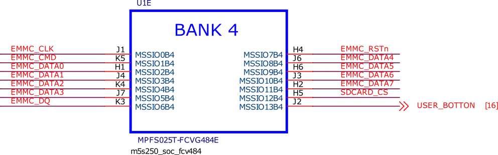
Fig. 262 SoC bank4
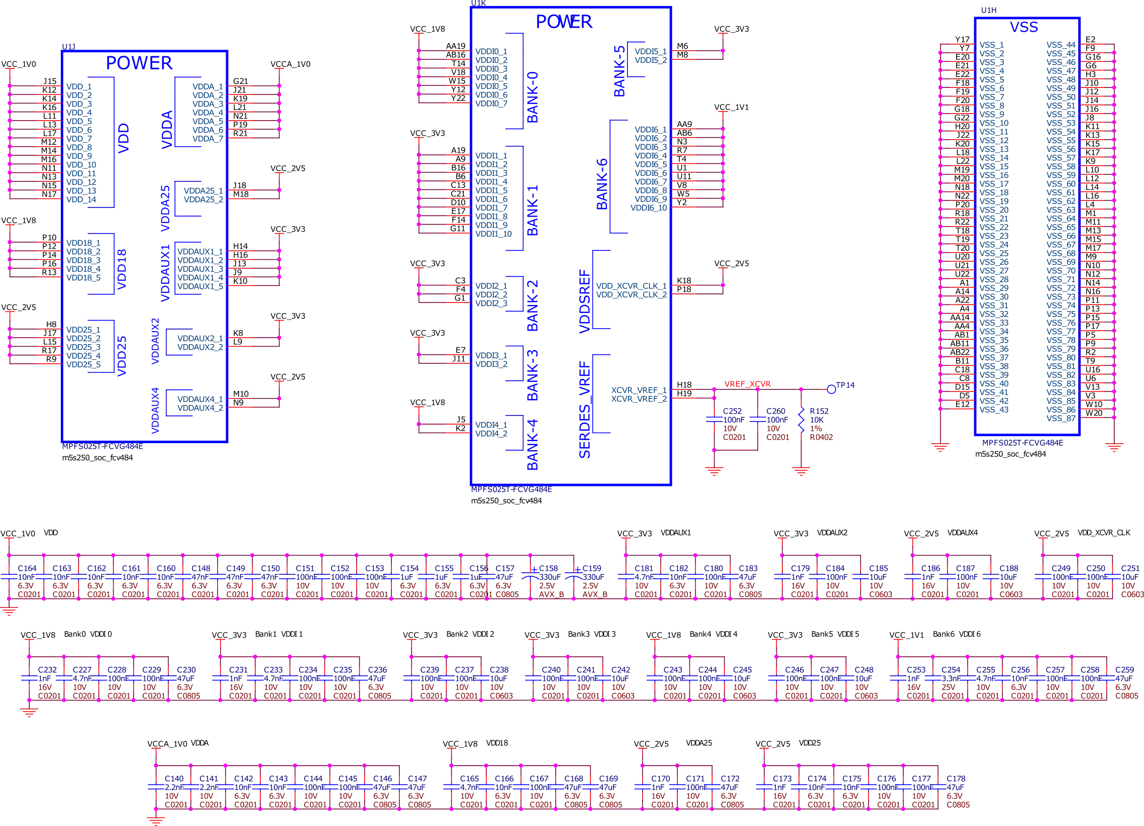
Fig. 263 SoC power
Power management
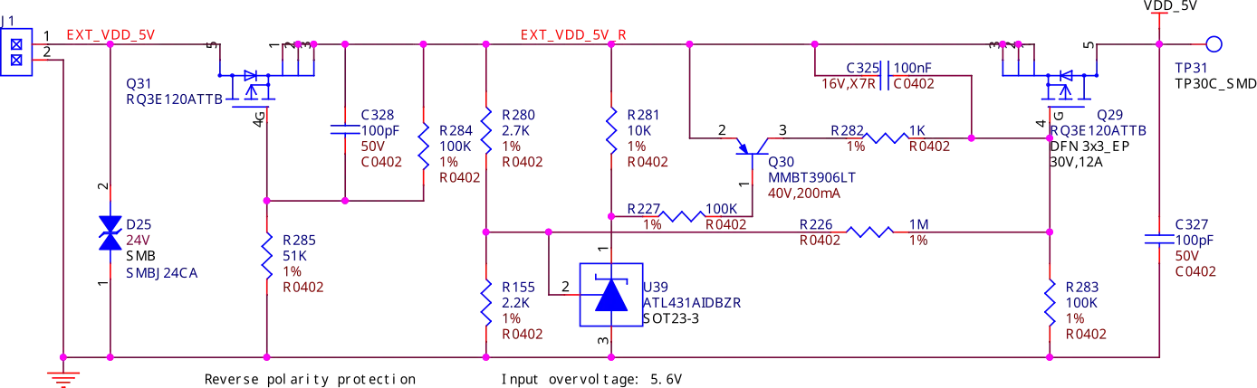
Fig. 264 DC 5V input
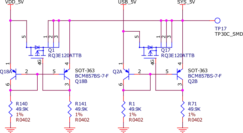
Fig. 265 Ideal diode
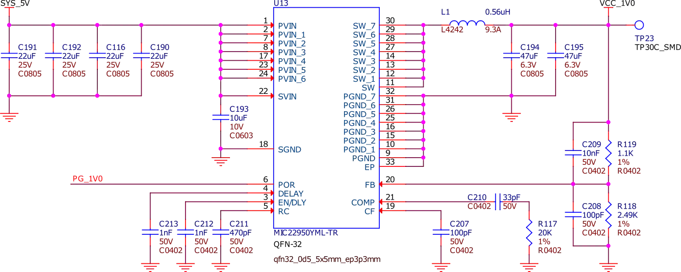
Fig. 266 VCC 1V0
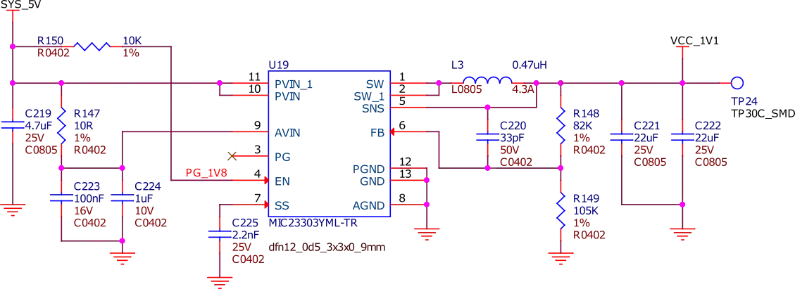
Fig. 267 VCC 1V1
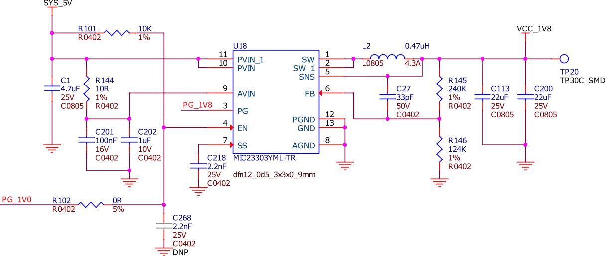
Fig. 268 VCC 1V8
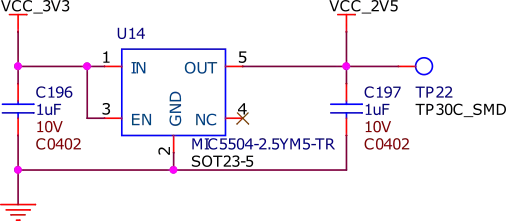
Fig. 269 VCC 2V5
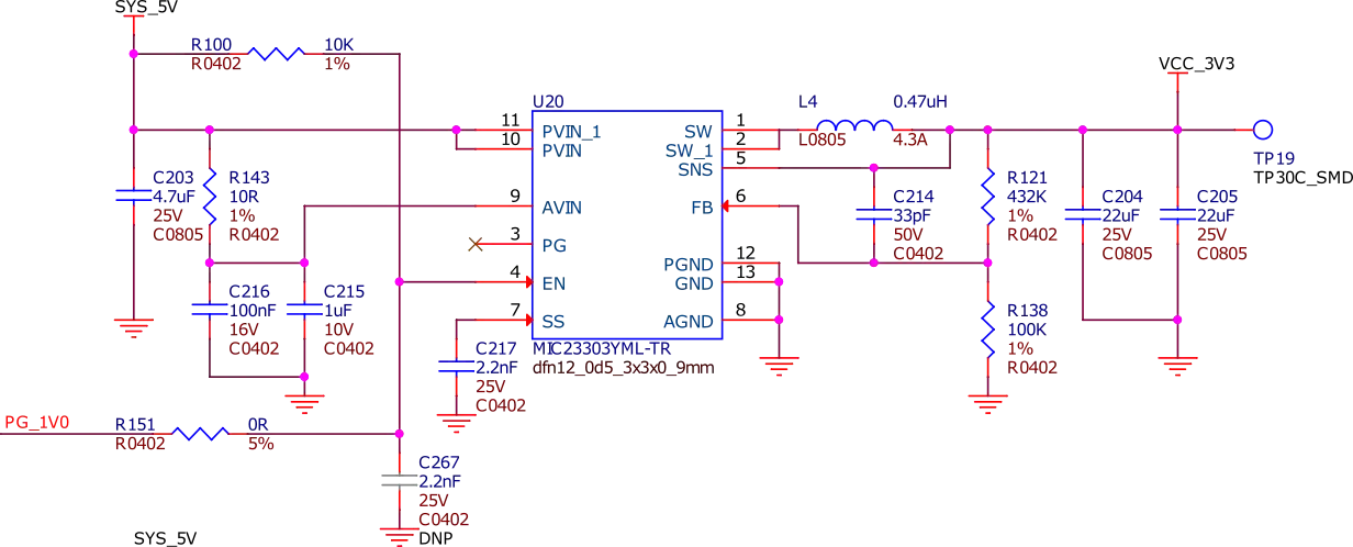
Fig. 270 VCC 3V3
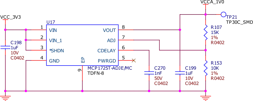
Fig. 271 VCCA 1V0
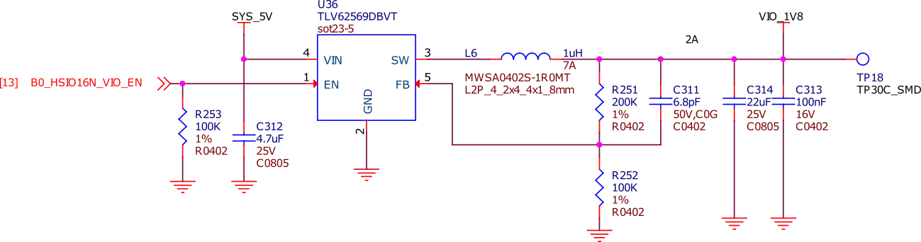
Fig. 272 VIO enable
General Connectivity and Expansion
USB-C port
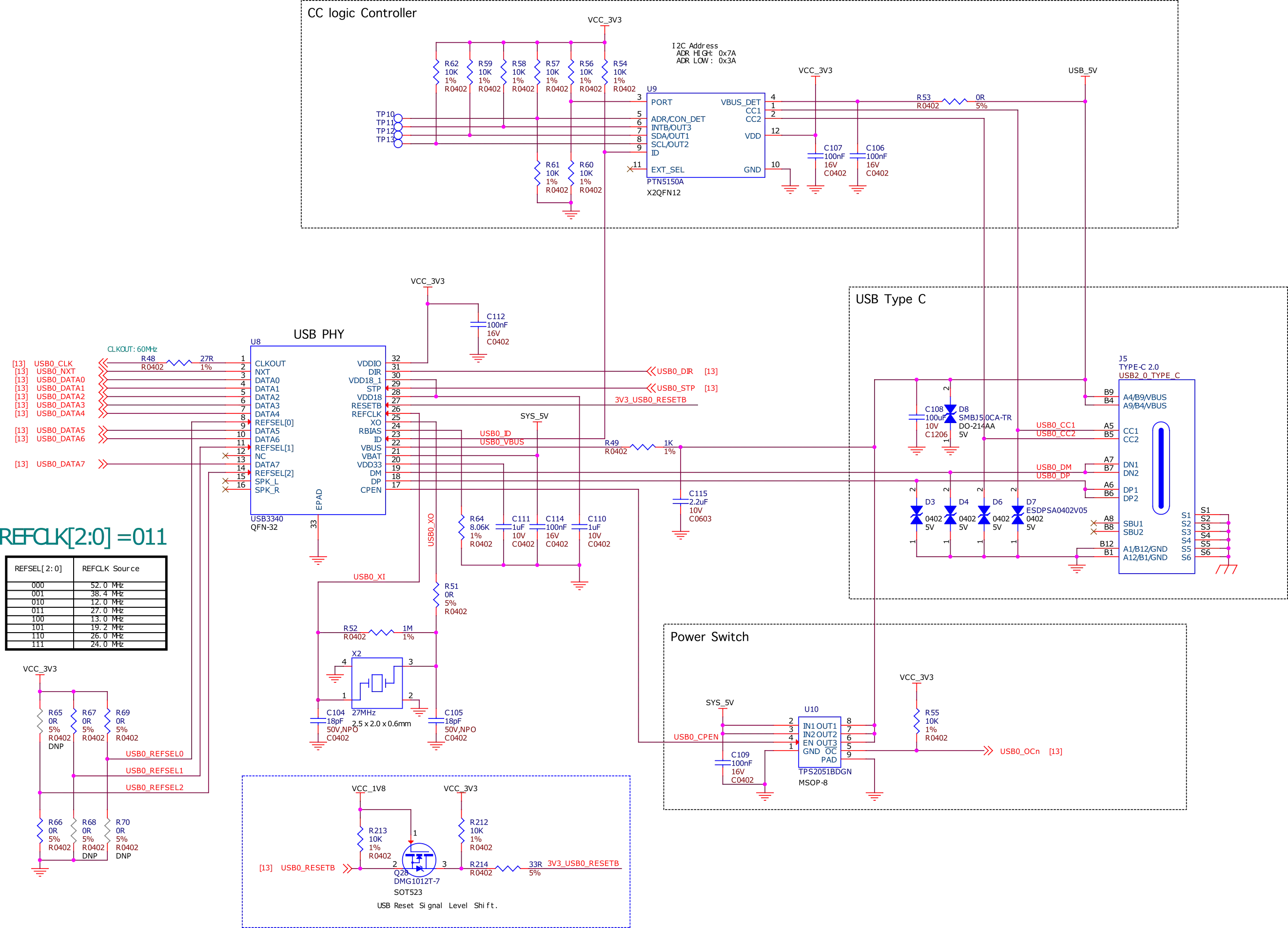
Fig. 273 USB C
P8 & P9 cape header pins
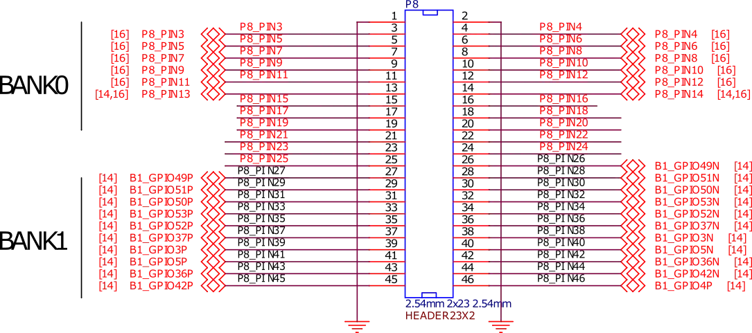
Fig. 274 P8 cape header
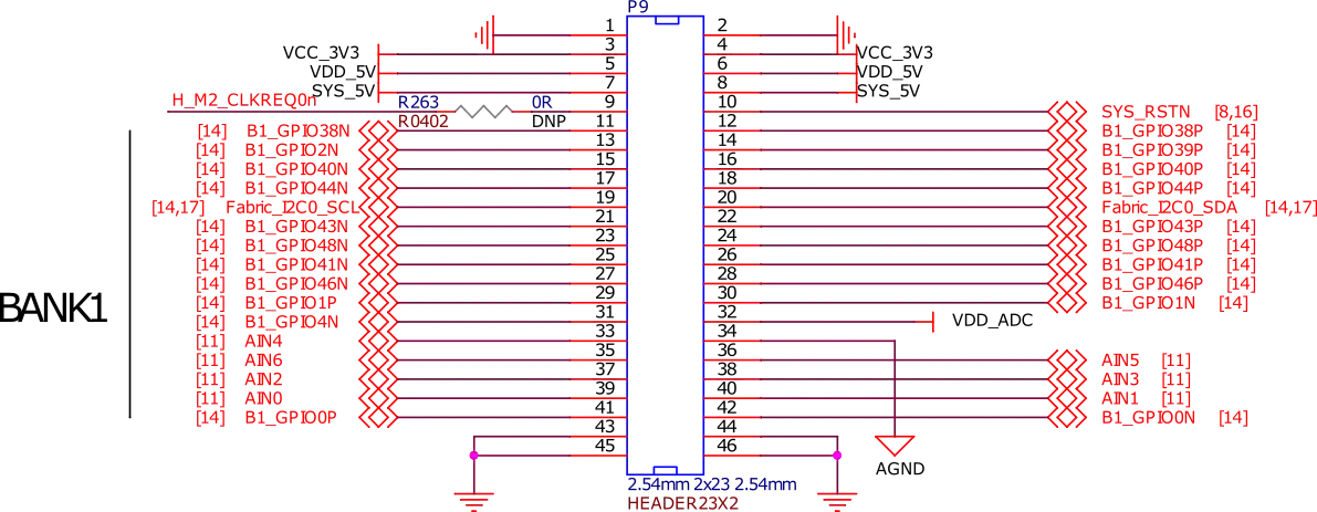
Fig. 275 P9 cape header
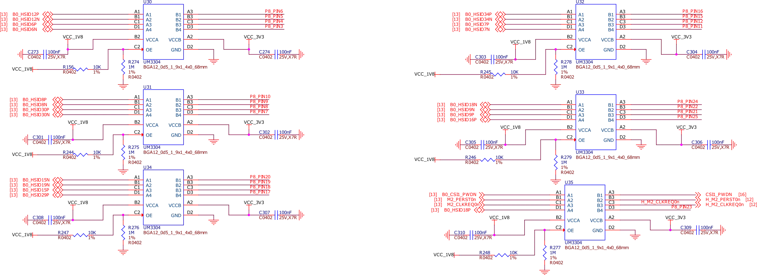
Fig. 276 Cape header voltage level translator
ADC
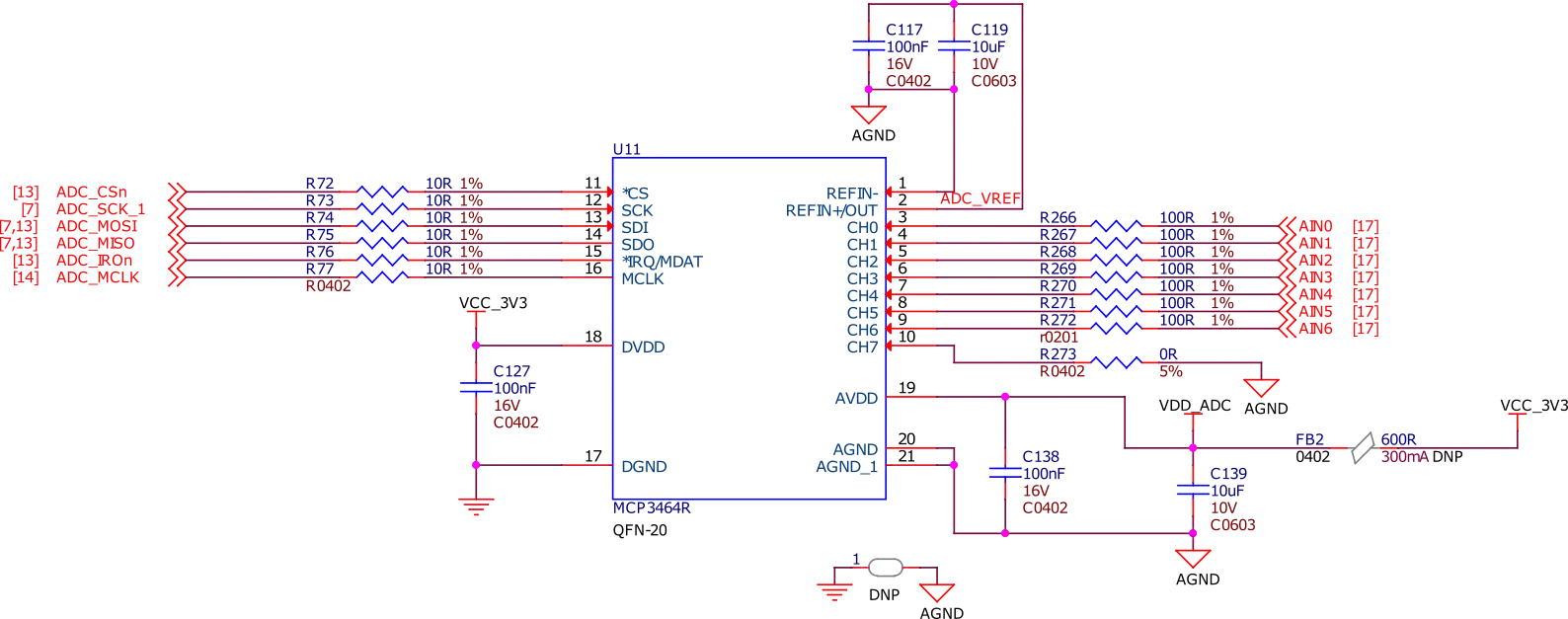
Fig. 277 16bit Delta-Sigma ADC
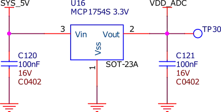
Fig. 278 ADC LDO power supply
Buttons and LEDs
User LEDs and Power LED
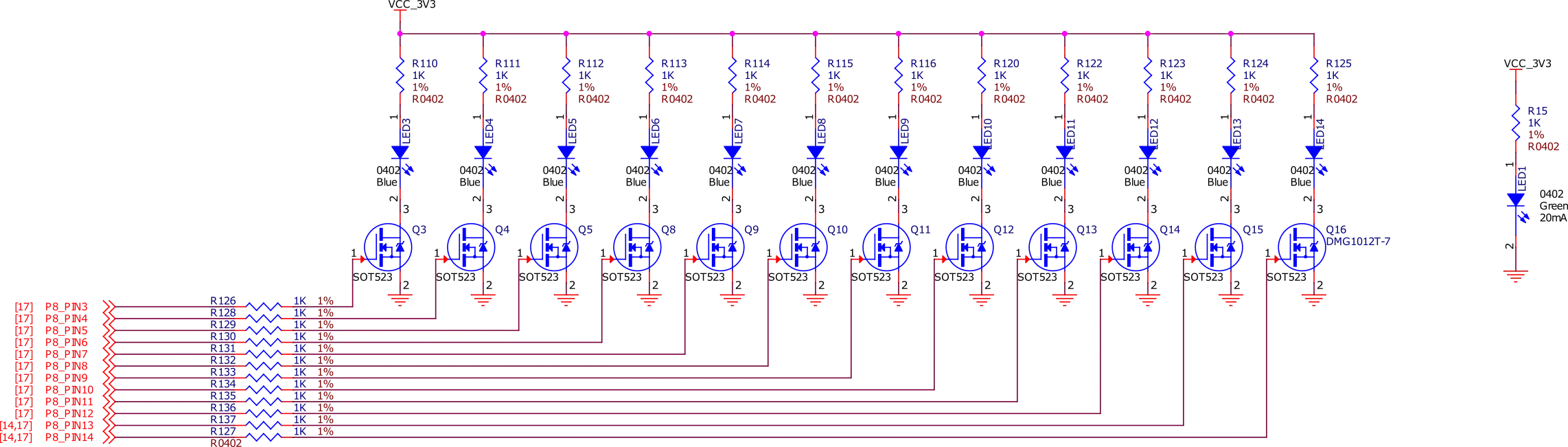
Fig. 279 User LEDs and power LED
User and reset button
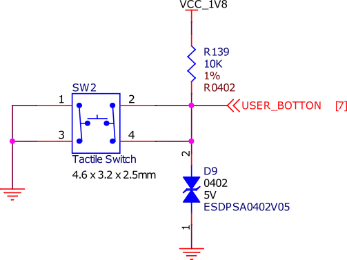
Fig. 280 User button
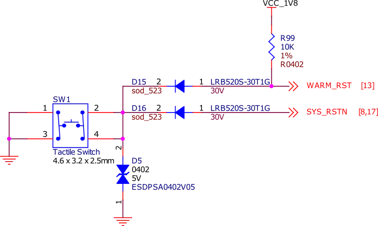
Fig. 281 Reset button
Connectivity
Ethernet
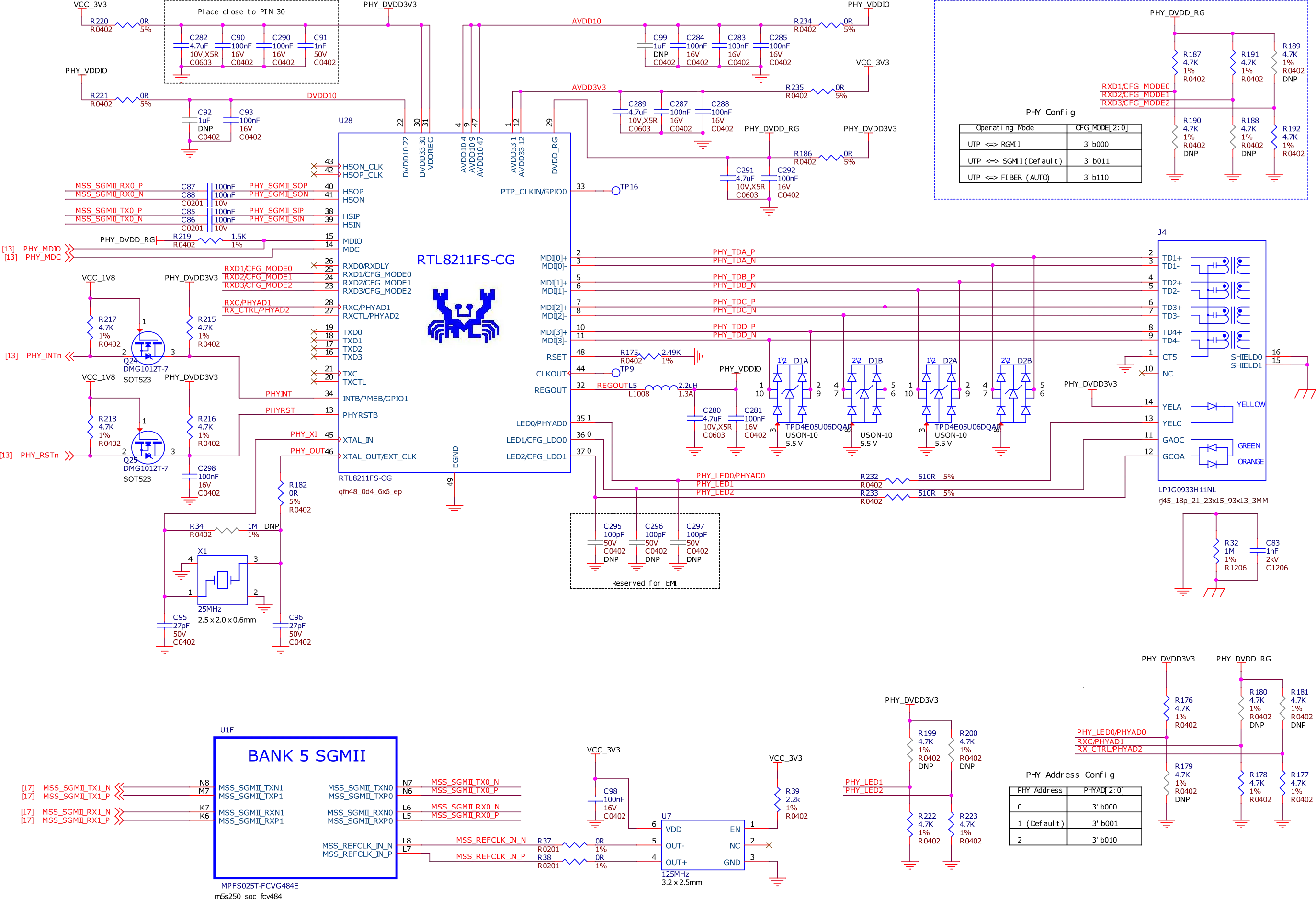
Fig. 282 Gigabit ethernet
Memory, Media and Data storage
DDR memory
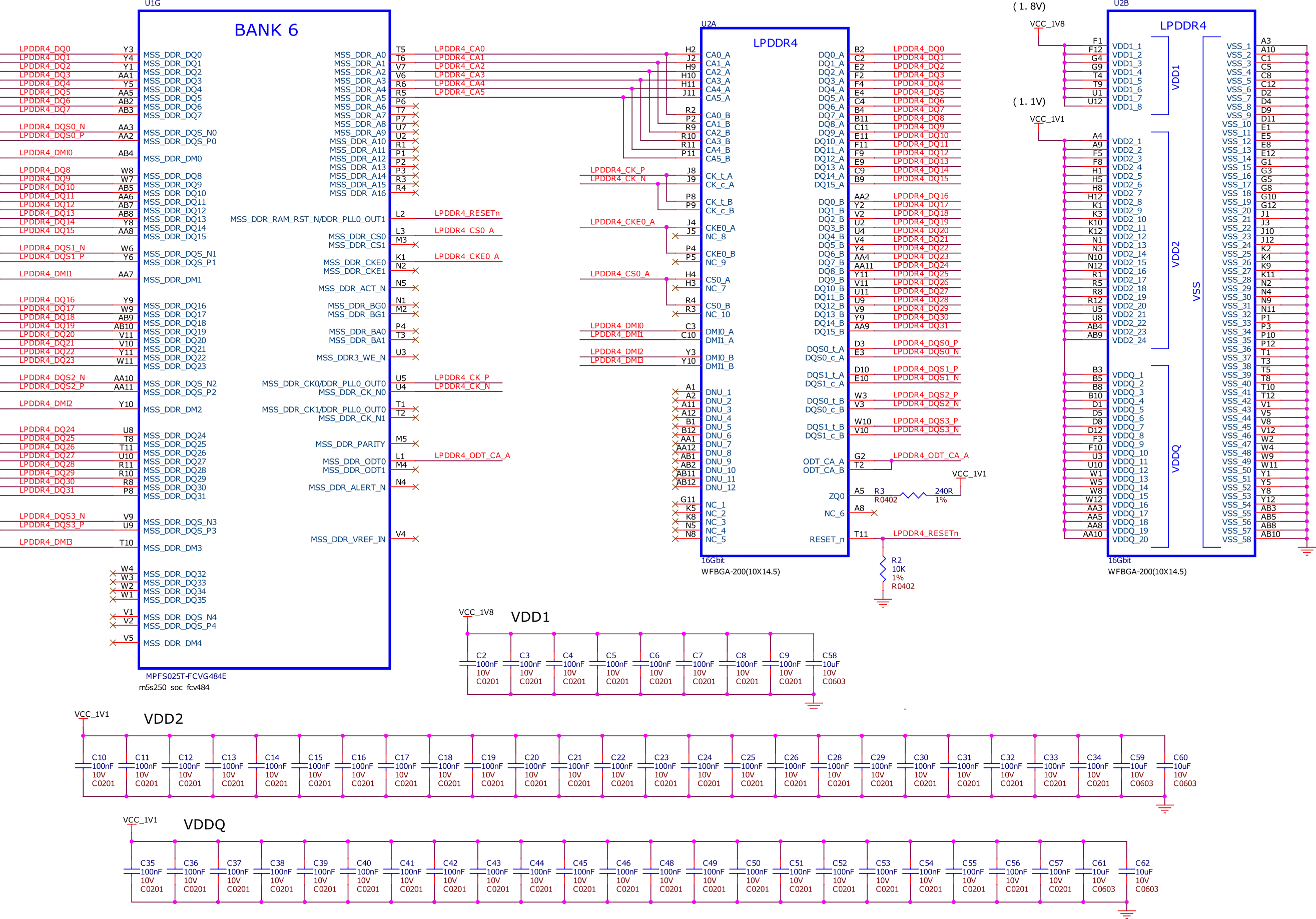
Fig. 283 LPDDR memory
eMMC
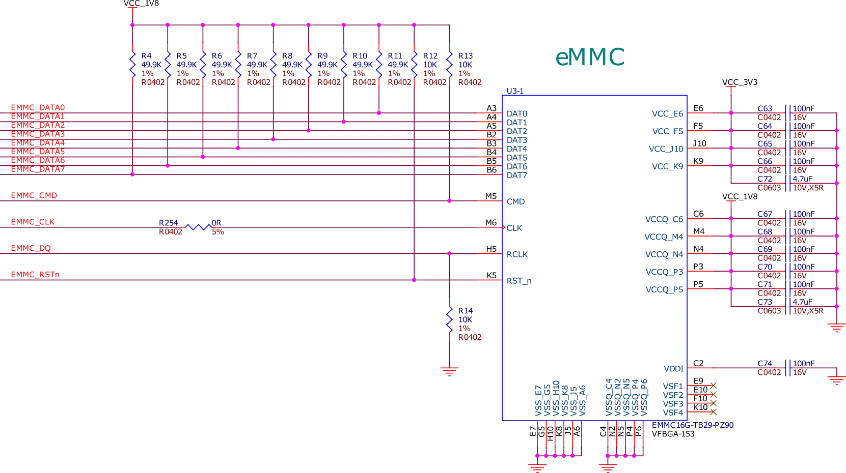
Fig. 284 EMMC flash storage
microSD
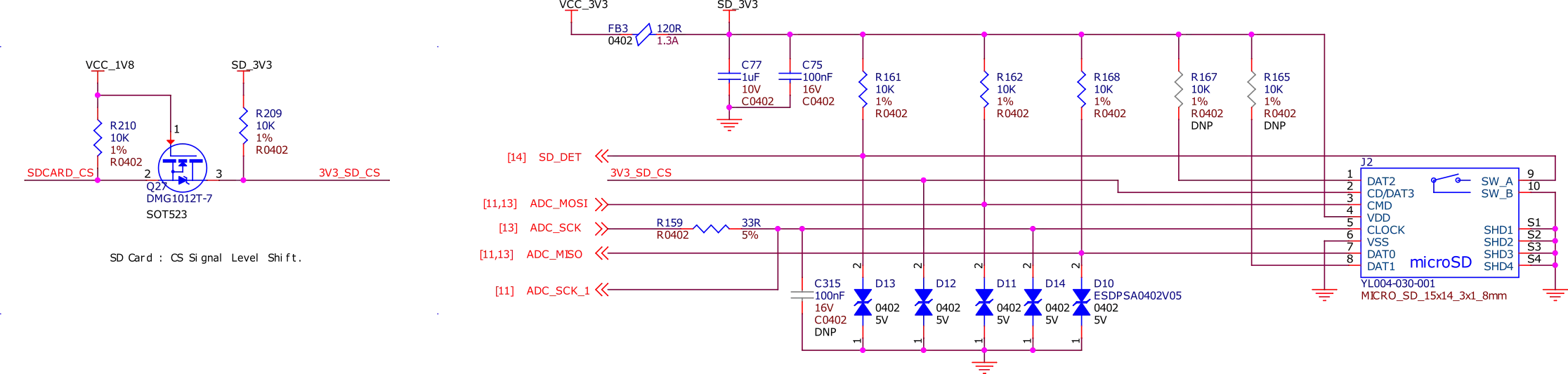
Fig. 285 SD Card socket
EEPROM
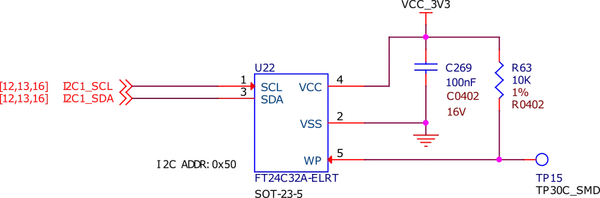
Fig. 286 EEPROM
SPI flash
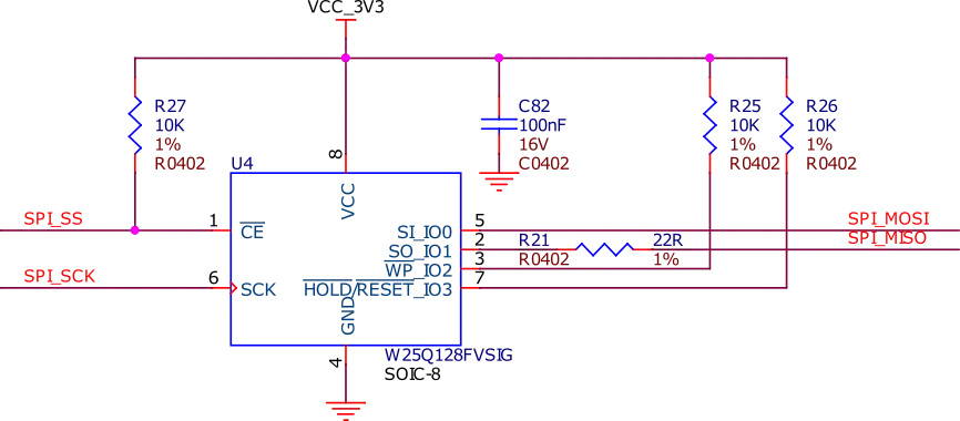
Fig. 287 SPI Flash
Multimedia I/O
CSI
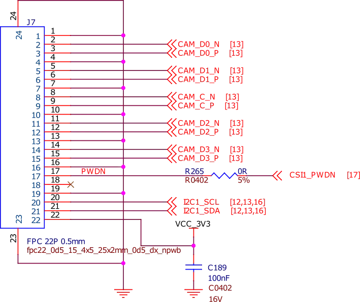
Fig. 288 CSI
Debug
UART debug port
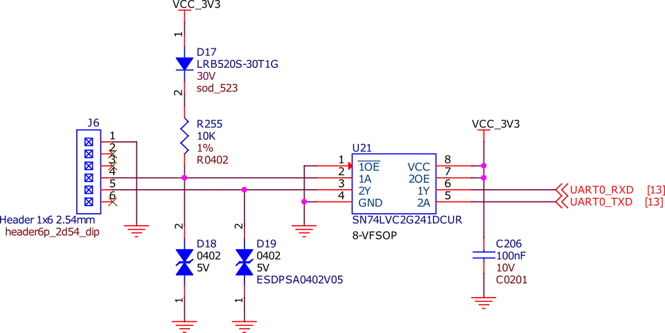
Fig. 289 UART debug header
JTAG debug port
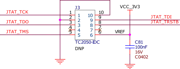
Fig. 290 JTAG debug header
Mechanical Specifications
Parameter |
Values |
|---|---|
Size |
86.38 * 54.61 * 18.8 mm |
Max heigh |
18.8 mm |
PCB Size |
86.38 * 54.6 mm |
PCB Layers |
12 Layers |
PCB Thickness |
1.6 mm |
RoHS compliant |
Yes |
Gross Weight |
106 g |
Net weight |
45.8 g |